Linear Regulators
The linear regulators are the original form of the regulating power supply. It relies upon the variable conductivity of an active electronics devices to drop voltage from an input voltage to a regulated output voltage. Linear regulators waste lot of power in the form of heat, and therefore gets hot. Linear regulators have an average efficiency of between 35% and 50%. It can only produce output voltage lower than their input voltage and can produce only one output voltage.
The linear regulators are useful for those application requiring less than 10W of output power. Above 10W, the heatsink required becomes so large and expensive that a switching power supply become more useful.
Linear Regulator Operation
Linear regulators use a closed feedback which hold the output voltage at a constant value. Linear regulators are step-down regulators only; the input voltage source must be higher than the desired output voltage.
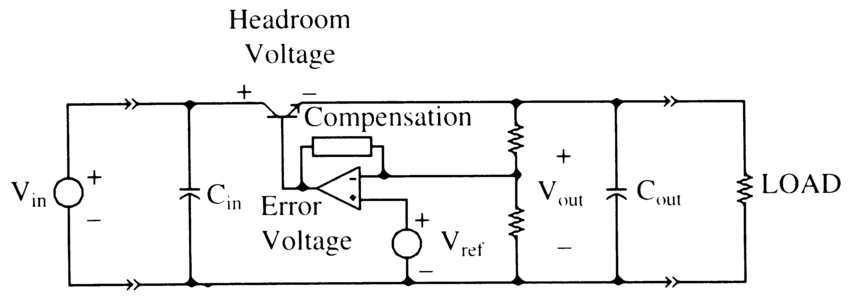
There are two types of linear regulators.
• The shunt regulators
• The series-pass regulators
The shunt regulators are a voltage regulator that is placed in parallel with the load. An unregulated current source is connected to a higher voltage source, the shunt regulators draws output current to maintain constant voltage across the load. A common example is Zener diode regulator.
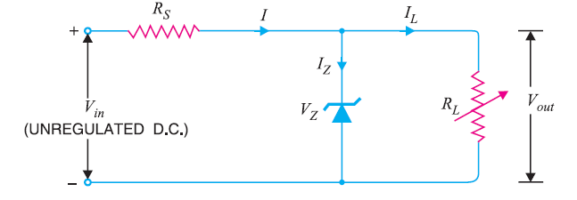
This type of regulation is needed when the voltage regulation is less than 200mW. A series resistance is placed to limit the current to the load and Zener diode. The Zener diode compensates for the variation in load current.
The series-pass linear regulator is more efficient than the shunt regulators and uses an active semiconductor as the series-pass unit between the input source and the load. It operates in the linear mode, which means that the unit is not designed to operate in the full on or off mode but instead operates in degree of “partially on”.
The heart of the negative feedback loop is high-gain operational amplifier called a voltage error amplifier. It continuously compares the difference between a very stable voltage reference and the output voltage. If the voltage is differing by mere millivolts, then a correction to the pass unit’s conductivity is made. A stable voltage reference is place on the noninverting input and is usually less than the output voltage. The output voltage is divided down to the level of the voltage reference. This divided output voltage is placed into the inverting input of operational amplifier. So, at the rated output voltage, the centre node of the output voltage divider is identical to the reference voltage.
The gain of the error amplifier produces a voltage that represent the greatly amplified difference between the reference and output voltage. The error voltage directly controls the conductivity of the pass unit thus maintaining the rated output voltage. If the load increase, the output voltage will fall. This will then increase the amplifier’s output, thus providing more current to the load. Similarly, if the load decrease, the output voltage will rise, thus making the error amplifier respond by decreasing pass unit current to the load.
The one-transistor series-pass linear regulator
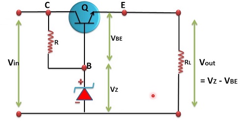
Adding a transistor to the basic Zener regulator we can increase the current limit of the regulator by using the gain of the BJT. The transistor is working as an emitter follower, which now can provide higher current to the load, and Zener current can be lowered. When the load current increases, it places a higher voltage into the base, which increases it conductivity, thus restoring the voltage to its original level.
Three-Terminal regulators Design
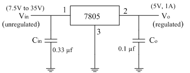
This example will illustrate the design consideration that should be undertaken with each 3-terminal regulator design. While designing we should consider the junction temperature profile, the heatsinks determines the regulator’s maximum output current.
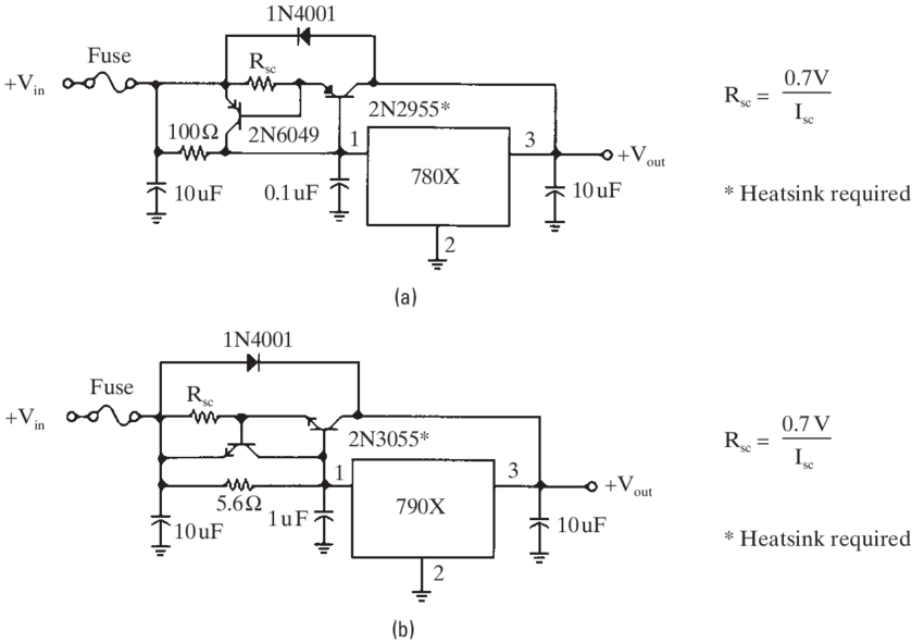
The 1N4001 is required for discharging the 100uF capacitor when the system is turned off.

The current-boosted regulator
Adding a transistor to the 3 terminal regulators will provide more current to the load. For negative Regulators, the power transistor will change from PNP to NPN.

The current-boosted 3 terminal regulator with overcurrent protection
By using this design, we can protect our IC from over current. It employs the base-emitter (0.6V) Junction of a transistor to accomplish the overcurrent threshold and gain of the overcurrent stage.
Linear regulator design Considerations
The majority use of linear regulators is in board level, low power application. The 3 terminal regulators are used in these circuits.
The first consideration is headroom voltage. It is the actual voltage drop between the input voltage and the output voltage during operation.
The second major consideration is dropout voltage. This voltage is the minimum headroom voltage that can be experienced by the linear regulator, below which it falls out of regulation.
Reference
If you are thinking to design your own power supply please Read this beautiful book “Power Supply cookbook” by “Marty Brown” before design. I had tried to highlight some of the points from the same book, hope you like it.